November 04, 2020
2278
Who invented PCB?

The creator of PCB is Austrian Paul Eisler (Paul Eisler), in 1936, he first used a printed circuit board in the radio. In 1943, Americans mostly used this technology for military radios. In 1948, the United States officially approved this invention for commercial use. Since the mid-1950s, printed circuit boards have been widely used.
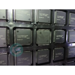
PCBs are ubiquitous and are widely used in communications, medical, industrial control, automotive, military, aviation, aerospace, consumer and other industries. In all kinds of electronic products, PCB, as the main part of product hardware, plays an indispensable role.
Why is PCB green?
If you are careful, you may find that most PCBs are green (there are fewer PCBs in black, blue, red, etc.). Why? In fact, the circuit board itself is brown, and the green we see is the solder mask. The solder mask is not necessarily green, there are red, yellow, blue, purple, black, etc., but green is the most common.
As for why the green solder mask is used, there are mainly the following statements:
1) Green is less irritating to eyes. Since childhood, the teacher told us that green is good for eyes, protects eyes and resists fatigue. The production and maintenance personnel are not prone to eye fatigue when staring at the PCB board for a long time, and the eyes are less harmful.
2) Lower cost. Since green is the mainstream in the production process, the purchase of natural green paint will be larger, and the purchase cost of green paint will be lower than other colors. At the same time, using the same color paint in mass production can also reduce the replacement cost.
3) When the board is soldered in SMT, it has to go through tinning, post filming and final AOI verification. These processes all need to be optically positioned and calibrated. The green background color is better for the recognition of the instrument.
How is the PCB designed?
To manufacture a PCB, the layout of the PCB must be designed first. PCB design needs to rely on EDA design software tools and platforms, such as Cadence Allegro, Mentor EE, Mentor Pads, Altium Designer, Protel, etc. At present, due to the continuous miniaturization, precision, and high speed of electronic products, PCB design not only needs to complete the circuit connection of various components, but also consider the various challenges brought by high speed and high density.
The basic process of PCB design is: preliminary preparation→PCB structure design→PCB layout design→PCB constraint setting and wiring design→wiring optimization and silk screen placement→network DRC inspection and structure inspection→PCB board manufacturing.
What are the white traces on the PCB?
We often see white printed lines on PCBs. Have you ever wondered what they are? These white printed lines are actually used to mark components and print important PCB information on the board, which is called "screen printing." It can be screen printed on the board, or printed on the PCB with an inkjet printer.
What are the components on the PCB?
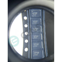
There are many individual components on the PCB, and each component has a different function, which together constitute the overall function of the PCB. The components on the PCB include resistors, potentiometers, capacitors, inductors, relays, batteries, fuses, transformers, diodes, transistors, LEDs, switches, etc.
Are there wires on the PCB?
Beginners may not know that the PCB is actually connected without wires. This is interesting because most electrical equipment and technologies require wires to be connected. There are no wires in the PCB, but copper traces are used to lead current to the entire device and connect all components.