February 21, 2024
8398
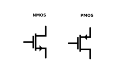
The field of electronics relies heavily on various types of transistors for signal processing, amplification, and switching purposes. Among these, NMOS (N-channel Metal-Oxide-Semiconductor) and PMOS (P-channel Metal-Oxide-Semiconductor) transistors are fundamental building blocks, forming the basis of many digital and analog circuits. Understanding the differences between NMOS and PMOS transistors, including their symbols, working principles, structures, and conduction characteristics, is essential for designing efficient and reliable electronic systems.
NMOS (N-channel Metal-Oxide-Semiconductor) is a type of field-effect transistor (FET). It's one of the two fundamental types of MOSFETs, the other being PMOS (P-channel Metal-Oxide-Semiconductor).
In an NMOS transistor, the channel through which current flows is created by applying a voltage to the gate terminal. This voltage creates an electric field which attracts electrons from the source terminal into the channel, allowing current to flow from the drain to the source when a sufficient voltage is applied between these two terminals.
NMOS transistors are extensively used in digital and analog circuits, such as in CMOS (Complementary Metal-Oxide-Semiconductor) technology, where they are paired with PMOS transistors to create complementary logic gates and complex integrated circuits. They are widely used in microprocessors, memory chips, and other digital logic circuits due to their high speed, low power consumption, and ease of integration into semiconductor manufacturing processes.
PMOS (P-channel Metal-Oxide-Semiconductor) is a type of field-effect transistor (FET) and one of the two fundamental types of MOSFETs, the other being NMOS (N-channel Metal-Oxide-Semiconductor).
In a PMOS transistor, the channel through which current flows is created by applying a voltage to the gate terminal. However, in PMOS transistors, the channel carries positively charged "holes" rather than electrons. When a voltage is applied to the gate terminal, it creates an electric field that repels holes away from the channel, allowing current to flow from the source to the drain when a sufficient voltage is applied between these two terminals.
PMOS transistors are commonly used alongside NMOS transistors in complementary metal-oxide-semiconductor (CMOS) technology. In CMOS circuits, PMOS transistors are used to implement the complementary logic functions to NMOS transistors, allowing for the construction of complex digital circuits with low power consumption and high noise immunity. PMOS transistors are utilized in various applications such as microprocessors, memory chips, and other integrated circuits.
In both symbols, the arrow indicates the direction of current flow when the transistor is conducting. The direction of the arrow for NMOS and PMOS transistors is opposite, reflecting the different types of charge carriers (electrons for NMOS and holes for PMOS) that constitute the channel when the transistor is in its conducting state.
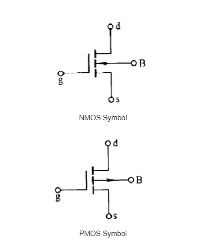
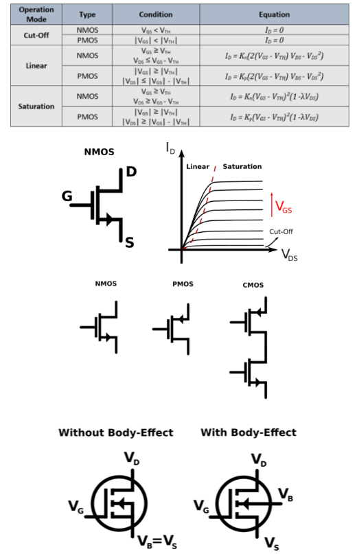
The working principles of NMOS (N-channel Metal-Oxide-Semiconductor) and PMOS (P-channel Metal-Oxide-Semiconductor) transistors are fundamentally similar but differ in the type of charge carriers they utilize and the direction of current flow.
When a positive voltage (logic HIGH) is applied to the gate terminal of an NMOS transistor with respect to the source, it creates an electric field that attracts electrons towards the interface between the gate and the semiconductor substrate.
This voltage creates an inversion layer or channel of n-type semiconductor material between the source and drain, allowing electrons to flow from the source to the drain when a voltage is applied across these terminals.
The transistor is said to be in the "ON" state when the gate voltage is sufficiently high to create the channel, allowing current to flow between the source and drain. Conversely, when the gate voltage is low (logic LOW), the transistor is in the "OFF" state, and negligible current flows between the source and drain.
In contrast, when a negative voltage (logic LOW) is applied to the gate terminal of a PMOS transistor with respect to the source, it creates an electric field that repels holes away from the interface between the gate and the semiconductor substrate.
This voltage creates a depletion region or channel of p-type semiconductor material between the source and drain, allowing holes to flow from the drain to the source when a voltage is applied across these terminals.
Similar to NMOS transistors, the PMOS transistor is in the "ON" state when the gate voltage is sufficiently low to create the channel, allowing current to flow between the source and drain. Conversely, when the gate voltage is high (logic HIGH), the transistor is in the "OFF" state, and negligible current flows between the source and drain.
In summary, NMOS transistors conduct current when a positive voltage is applied to the gate, while PMOS transistors conduct current when a negative voltage is applied to the gate. This fundamental difference in operation allows NMOS and PMOS transistors to complement each other in CMOS (Complementary Metal-Oxide-Semiconductor) technology, enabling the construction of various digital logic circuits and integrated circuits.
The structure of NMOS (N-channel Metal-Oxide-Semiconductor) and PMOS (P-channel Metal-Oxide-Semiconductor) transistors is similar in many respects, but they differ in terms of the type of semiconductor material used and the polarity of the majority charge carriers in their channels.
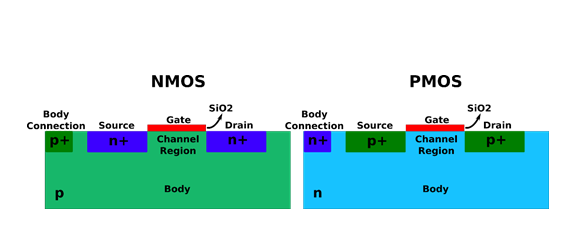
Substrate: Both NMOS and PMOS transistors are typically fabricated on a silicon substrate.
Gate: Both types of transistors have a gate terminal made of a conductive material such as polysilicon. The gate is insulated from the semiconductor substrate by a thin layer of insulating material (usually silicon dioxide) known as the gate oxide.
Source and Drain: These are the terminals through which current enters and exits the transistor channel. In NMOS transistors, electrons flow from the source to the drain (hence the name "N-channel"), while in PMOS transistors, holes flow from the drain to the source (hence the name "P-channel"). The source and drain regions are doped with impurities to create the desired conductivity type (n-type for NMOS, p-type for PMOS).
Channel: The channel is the region between the source and drain terminals that is controlled by the voltage applied to the gate. In NMOS transistors, the channel consists of an n-type semiconductor material, allowing electrons to flow when a voltage is applied to the gate. In PMOS transistors, the channel consists of a p-type semiconductor material, allowing holes to flow when a voltage is applied to the gate.
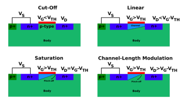
Overall, the key structural difference between NMOS and PMOS transistors lies in the polarity of the majority charge carriers in their channels, which dictates the direction of current flow and the type of doping used in the source and drain regions.
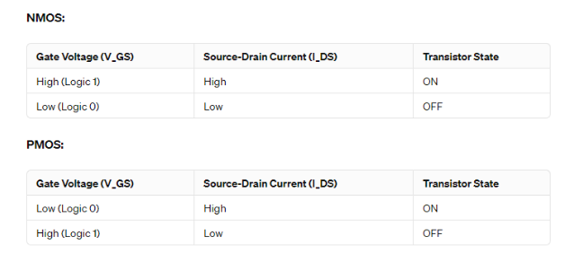
In both tables:
"Gate Voltage (V_GS)" refers to the voltage applied to the gate terminal with respect to the source terminal.
"Source-Drain Current (I_DS)" indicates whether current can flow from the source to the drain terminals.
"Transistor State" specifies whether the transistor is in the ON state (conducting) or the OFF state (non-conducting).
For NMOS transistors, the transistor conducts (ON) when the gate voltage is high (Logic 1), allowing current to flow from the source to the drain. Conversely, when the gate voltage is low (Logic 0), the transistor is off, and no significant current flows.
For PMOS transistors, the transistor conducts (ON) when the gate voltage is low (Logic 0), allowing current to flow from the drain to the source. When the gate voltage is high (Logic 1), the transistor is off, and negligible current flows.
The conduction characteristics of NMOS (N-channel Metal-Oxide-Semiconductor) and PMOS (P-channel Metal-Oxide-Semiconductor) transistors differ primarily in terms of the type of charge carriers they utilize and the direction of current flow.
Operation: Conducts when a positive voltage is applied to the gate terminal relative to the source terminal.
Charge Carriers: Utilizes electrons as majority charge carriers.
Channel Creation: Application of a positive gate-source voltage attracts electrons towards the interface between the gate and the semiconductor substrate, creating an inversion layer or channel of n-type semiconductor material.
Current Flow: Current flows from the source to the drain terminals, as electrons move through the channel under the influence of the electric field applied by the gate voltage.
Operation: Conducts when a negative voltage is applied to the gate terminal relative to the source terminal.
Charge Carriers: Utilizes holes as majority charge carriers.
Channel Creation: Application of a negative gate-source voltage repels holes away from the interface between the gate and the semiconductor substrate, creating a depletion region or channel of p-type semiconductor material.
Current Flow: Current flows from the drain to the source terminals, as holes move through the channel under the influence of the electric field applied by the gate voltage.
In summary, NMOS and PMOS transistors exhibit opposite conduction characteristics due to the polarity of the majority charge carriers in their channels and the direction of current flow when they are in the conducting state.
In terms of MOS switch tube loss, the key factor to consider is the resistance of the transistor when it is fully turned on. This resistance contributes to the losses in the switch when it conducts current. Here's how NMOS and PMOS transistors compare in this regard:
Typically exhibits lower on-resistance (R_ds(on)) when fully turned on compared to PMOS transistors.
Due to the mobility of electrons being typically higher than that of holes in semiconductor materials, NMOS transistors tend to have lower resistance in their conducting state.
Lower on-resistance leads to lower conduction losses in NMOS switches when they are fully turned on, resulting in higher efficiency.
May have higher on-resistance (R_ds(on)) when fully turned on compared to NMOS transistors.
Due to the lower electron mobility compared to hole mobility in semiconductor materials, PMOS transistors often have higher resistance in their conducting state.
Higher on-resistance can result in higher conduction losses in PMOS switches when they are fully turned on, potentially leading to slightly lower efficiency compared to NMOS switches.
In practical applications, the choice between NMOS and PMOS switches depends on various factors such as the specific requirements of the circuit, including voltage levels, current levels, switching speed, and overall system efficiency. However, for high-frequency and high-efficiency applications, NMOS switches are often preferred due to their lower on-resistance and lower conduction losses.
In digital circuit design, MOS (Metal-Oxide-Semiconductor) transistors, including both NMOS (N-channel MOS) and PMOS (P-channel MOS), are commonly used as driver transistors to control the switching behavior of other MOS devices or to provide the driving force for the signal lines. Here's how NMOS and PMOS transistors compare as MOS tube drivers:
NMOS transistors are often used as pull-down (ground-connected) drivers in CMOS (Complementary MOS) circuits.
When a logic HIGH voltage is applied to the gate of an NMOS transistor, it turns off the transistor, allowing the signal line to be pulled to ground through a low-resistance path, effectively driving the line low.
NMOS drivers are suitable for driving signals or loads that require a strong connection to ground.
In CMOS logic circuits, NMOS transistors are typically used for switching and amplifying signals on the low side of the circuit.
PMOS transistors are commonly used as pull-up (VDD-connected) drivers in CMOS circuits.
When a logic LOW voltage is applied to the gate of a PMOS transistor, it turns off the transistor, allowing the signal line to be pulled to the supply voltage (VDD) through a low-resistance path, effectively driving the line high.
PMOS drivers are suitable for driving signals or loads that require a strong connection to the supply voltage.
In CMOS logic circuits, PMOS transistors are typically used for switching and amplifying signals on the high side of the circuit.
In CMOS technology, NMOS and PMOS transistors are often used together to form complementary pairs, where one type of transistor handles pull-up operations while the other handles pull-down operations. This complementary configuration allows for efficient and low-power operation in CMOS logic circuits. The choice between NMOS and PMOS drivers depends on the specific requirements of the circuit, such as voltage levels, signal characteristics, and power consumption considerations.
The difference between NMOS and PMOS biasing lies in how the substrate, or body, of the transistor is biased relative to the power supply voltage (Vdd for PMOS and Vss for NMOS) in order to reduce leakage currents and improve overall device performance.
In PMOS biasing, the substrate biasing (also known as back biasing) biases the body of the PMOS transistor to a voltage higher than the power supply voltage (Vdd).
By biasing the substrate to a voltage higher than Vdd, the threshold voltage (Vth) of the PMOS transistor is effectively increased. This helps to reduce leakage currents, as the transistor becomes less likely to conduct when it's supposed to be in the off state.
The higher substrate bias voltage in PMOS helps to enhance the transistor's performance by minimizing leakage currents and improving overall power efficiency.
In contrast, in NMOS biasing, the substrate biasing biases the body of the NMOS transistor to a voltage lower than the ground potential (Vss).
By biasing the substrate to a voltage lower than Vss, the threshold voltage (Vth) of the NMOS transistor is effectively decreased. This reduces leakage currents, as the transistor becomes less likely to conduct when it's supposed to be in the off state.
The lower substrate bias voltage in NMOS helps to minimize leakage currents and improve the efficiency of the transistor.
In summary, while both NMOS and PMOS biasing techniques aim to reduce leakage currents by adjusting the substrate bias voltage, they do so in opposite ways due to the inherent differences in their operation. PMOS biasing involves biasing the substrate to a voltage higher than Vdd, while NMOS biasing involves biasing the substrate to a voltage lower than Vss. These techniques help to optimize transistor performance and minimize power consumption in integrated circuit designs.
These are just a few examples of MOS transistor models with their voltage ratings, current ratings, and on-resistance values. The selection of a specific MOS transistor depends on the application requirements such as voltage, current, power dissipation, and package type.
A2700 (Surface Mount)
Voltage Rating: 30V
Current: 9A
On-Resistance: 7.3mΩ
SI4336 (Surface Mount)
Voltage Rating: 30V
Current: 22A
On-Resistance: 4.2mΩ
SI4404 (Surface Mount)
Voltage Rating: 30V
Current: 17A
On-Resistance: 8mΩ
SI4410 (Surface Mount)
Voltage Rating: 30V
Current: 10A
On-Resistance: 14mΩ
IRF7831 (Surface Mount)
Voltage Rating: 30V
Current: 16A
On-Resistance: 0.004Ω
A2716 (Surface Mount)
Voltage Rating: 30V
Current: 7A
On-Resistance: 11.3mΩ
SI4405 (Surface Mount)
Voltage Rating: 30V
Current: 17A
On-Resistance: 7.5mΩ
SI4425 (Surface Mount)
Voltage Rating: 30V
Current: 9A
On-Resistance: 19mΩ
IRF7424 (Surface Mount)
Voltage Rating: 30V
Current: 8.8A
On-Resistance: 22mΩ
BTS120 (Through Hole)
Voltage Rating: 100V
Current: 19A
On-Resistance: 100mΩ
In conclusion, the comparison between NMOS and PMOS transistors reveals their complementary roles in electronic circuit design. NMOS transistors, utilizing electrons as majority charge carriers, excel in pull-down operations and are widely used for low-side switching. On the other hand, PMOS transistors, which utilize holes as majority charge carriers, are suitable for pull-up operations and find applications in high-side switching. The combination of NMOS and PMOS transistors in CMOS technology enables the development of complex digital systems with low power consumption and high performance. As technology continues to advance, the distinct characteristics of NMOS and PMOS transistors will continue to play a crucial role in shaping the future of electronics.