September 13, 2021
2613
The whole process of chip manufacturing includes chip design, chip manufacturing, packaging manufacturing, testing and so on. The chip manufacturing process is particularly complicated.
The first is chip design. According to the design requirements, "patterns" are generated
1. Wafer material
The component of the silicon wafer is silicon, which is refined from quartz sand. The silicon wafer is purified by silicon element (99.999%) and made into silicon rods, which become the quartz semiconductor material for manufacturing integrated circuits. A chip is a specific wafer required for chip manufacturing. The thinner the wafer, the lower the production cost, but the higher the process requirements.
2. Wafer coating
Wafer coating can resist oxidation and temperature, and its material is a photoresist.
3. Wafer photolithography development and etching
First, a layer of photoresist is applied to the surface of the wafer (or substrate) and dried. The dried wafer is transferred to the lithography machine. Through the mask, light projects the pattern on the mask onto the photoresist on the surface of the wafer to achieve exposure and chemiluminescence reactions. The exposed wafer is subjected to secondary baking, the so-called post-exposure baking, and the photochemical reaction after baking is more sufficient.
Finally, the developer is sprayed on the photoresist on the wafer surface to form an exposure pattern. After development, the pattern on the mask remains on the photoresist. Gelatinization, baking and development are all done in a homogeneous developer, and exposure is done in a lithographic printing machine. The homogenization developing machine and the lithography machine are generally operated online, and the wafer is transferred between the units and the machine by a robot.
The entire exposure and development system is closed, and the wafer is not directly exposed to the surrounding environment to reduce the impact of harmful components in the environment on the photoresist and photochemical reactions.

4. Add impurities
The corresponding p and n semiconductors are formed by implanting ions into the wafer.
The specific process is to start from the exposed area on the silicon wafer and put it into the chemical ion mixture. This process will change the conduction mode of the doped region so that each transistor can be turned on, off, or carry data. A simple chip can only use one layer, but a complex chip usually has many layers.
At this point, the process repeats continuously, and different layers can be connected by opening a window. This is similar to the manufacturing principle of multilayer PCBs. More complex chips may require multiple silicon dioxide layers. At this time, it is achieved by repeating the photolithography and the above process to form a three-dimensional structure.
5. Wafer
After the above processing, lattice-shaped crystal grains are formed on the wafer. The electrical properties of each crystal grain were tested by the needle method. Generally speaking, each chip has a large number of crystal grains, and organizing a pin test mode is a very complicated process, which requires mass production of chips of the same specification and model as much as possible. The larger the number, the lower the relative cost, which is also a factor in the low cost of mainstream chip equipment. 6. Package
The same chip core can have different packaging forms, the reason is that the chip is fixed, the pins are bound, and different packaging forms are made according to the needs. For example: DIP, QFP, PLCC, QFN, etc., which mainly depends on the user's application habits, application environment, market shape and other external factors.
6. Testing and packaging
After the above process, chip production has been completed. This step is to test the chip, remove the defective product, and pack it.
What exactly is a transistor in a chip?
In short, a transistor is a variable resistor.
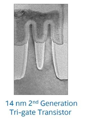
Explained in English, a transistor can be regarded as a combination of transfer-resistor. It is a device that regulates current or voltage and can switch or amplify signals as a basic element in integrated circuits. , An integrated circuit consists of a large number of transistors interconnected with the circuit. The transistors in the latest Intel CPUs look like this:

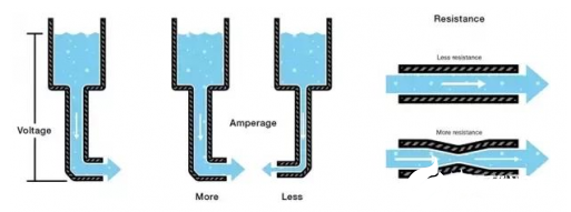
Maybe everyone is still looking dumbfounded. To make a simple analogy, current is like the flow of water, and voltage is the pressure of water. Under the same pipe diameter, the greater the water pressure, the greater the flow of water, and the same water pressure. The smaller the pipe diameter, the smaller the water flow (note that it is the flow, not the flow rate. Think about the time it takes to open the faucet and open a bucket of water. Obviously, it takes more time to open the faucet for hours).

Transistors are like water valves in water pipes and can be used to control the flow of mechanisms. This water valve usually has three states:
①Fully open-water does not flow any restrictions
②All off-completely stop the flow of water
③Flow control-control the opening and closing degree of the water valve so that the water flows at a certain flow rate
Transistors can do the same thing, linearly controlling the current in the circuit at some point between completely closed (open circuit) and completely open (short circuit). The size of the pipe diameter is similar to the resistance in the circuit. If a valve can accurately adjust the size of the pipe, then a transistor can accurately adjust the resistance between the two poles.
So, in a sense, the transistor is like a variable resistor.
As for how transistors are made, it is more than just a few words. Basically, the evolutionary journey of sand is also the most difficult manufacturing technology in chip technology.