January 04, 2021
3582
In the PCB design, when the final PCB mass production is carried out, the PCB assembly is also a very important matter, which not only involves the quality standards of the PCB circuit board, but also affects the cost of PCB production. It is a problem that the production company pays great attention to how to make reasonable and effective splicing under the premise of ensuring the quality of PCB circuit boards to save raw materials.
Imposition connection method:
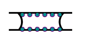
There are two ways to link PCB imposition, one is V-cut (as shown in the picture) and the other is the stamp hole link (as shown in the picture).
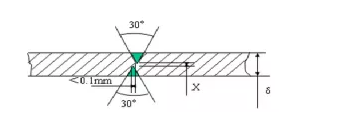
V-cut is generally suitable for PCBs with a rectangular shape. It is characterized by neat edges after separation and low processing cost. It is recommended to use it first, as shown in the figure;
Stamp holes are generally suitable for irregular plate imposition. For example, MID's "L"-shaped frame structure often uses the linking method of stamp holes for imposition.
Number of imposition:
The size of the entire imposition must be calculated based on the size of a single PCB board. The size of the entire imposition must not exceed the maximum size of the PCB (the PCB imposition length must not be greater than 250mm), and too many impositions will affect the accuracy of the imposition position and affect the placement accuracy. Generally, the main board of the MID type is 2 imposition, and the sub-board of the key board and LCD board does not exceed 6 pieces. The sub-board of the special area depends on the specific situation.
Requirements for the link strip of the stamp hole:
In the imposition of a PCB, the number of link bars should be appropriate, generally 2-3 link bars, so that the strength of the PCB meets the requirements of the production process, and it should not be broken at every turn.
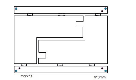
Craft side:
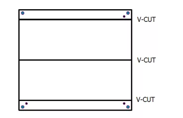
When the board is relatively dense with components and the board edge space is limited, it is necessary to increase the process edge. When used for SMT, the transfer edge of the PCB board is generally 3-5mm. Generally, a positioning hole is added to each of the four corners on the process side, and optical positioning points are added to the three corners to strengthen the positioning of the machine, as shown in the figure.