January 18, 2021
2556
The demand for higher density NAND flash memory continues to grow throughout the global storage market. At present, this demand has been met through many developments, not only the functions of today's flash memory controllers, but also the 3DNAND architecture in particular, which has been the center of storage discussion and development in the past decade.
As the Industrial Internet of Things (IIoT), smart factories, self-driving cars, and other data-intensive applications continue to receive attention, the requirements for data storage in these demanding applications have become increasingly challenging. Although there are still price advantages compared with traditional HDD, the development of 3D architecture expands flash storage to a wider market because of its higher scalability and affordability.
3D technology: floating gate and charge trap technology
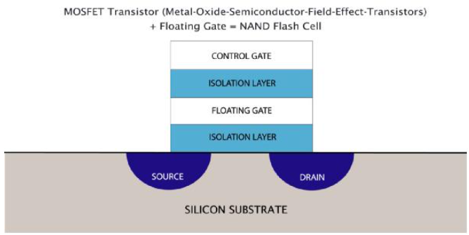
Since the introduction of the 2D flat landscape of SLC flash in the 1980s, flash drives have been using floating gate technology. 3D technology pushes things to three dimensions, and brings new challenges, and returning to programming techniques such as charge traps, vendors have begun to reconsider enterprise-level solid state drives. Although most 3D manufacturers have now turned to charge trap technology to achieve better durability and scalability, planar technology still mainly uses floating gate technology to store data.
Some people believe that NAND flash memory based on charge trap technology is not susceptible to physical damage and leakage. This directly affects the error rate and the remaining program/erase (P/E) cycles on the drive. However, especially at higher temperatures, charge traps also face their own challenges in data preservation. This is a very important issue in the automotive field, because the quality requirement standard is that it can withstand high temperatures.

Regardless of the charge trap technology or the floating gate technology, the data sent from any particular host system to the NAND flash memory needs to be managed by the flash memory controller. This is why highly reliable controllers are an integral part of high-performance systems. 3D architecture provides a way to achieve high-density flash memory, but storage applications based on this technology are now increasingly demanding higher levels of reliability and data preservation, which can only be achieved through high-end controllers. Ultimately, choosing a flash memory controller is the key to greater durability and longevity.
Why choose 3D technology: the economics of expansion
The economics of silicon manufacturing are based on the fact that the cost of processing wafers is fixed under a certain technological scale. Since smaller processes require different equipment, there are differences in processing costs. However, the cost of each silicon chip almost entirely depends on its size. In the end, the more devices that can be installed on the wafer, the lower the cost per chip. The economics of storage are mainly about reducing cost per bit. For storage devices, this means storing more bits on a chip of a certain size.
The obvious solution is to make the storage unit smaller. Flash memory has evolved from 120nm manufacturing to 14 or 15nm used today. This expansion increases the capacity by a factor of approximately 100 (thus reducing the cost per bit). However, our semiconductor manufacturing process is about to reach the limit of expansion.
Another method is to store more data bits in each memory cell. The original single-level cell becomes a multi-level cell (MLC), which stores four different levels of charge in each cell, which is equivalent to two data bits. Since then, flash memory has been designed to store three bits (three-level cell, TLC) and four bits (four-level cell, QLC) in each cell. There are some problems with this method: it requires more precise control and measurement of the stored charge, which makes reading and writing speeds a little slower and more prone to errors. However, the increase in density and the corresponding reduction in cost per bit make it quite cost-effective in some applications.
In order to meet the demand for increased storage density, flash memory manufacturers have now entered the three-dimensional field. In the 3D architecture, multi-layer memory cells are built in silicon to create a three-dimensional structure. This can provide more storage space for the same surface area. The 3D architecture is fabricated by building cell layers vertically in silicon. This requires a more complex process, but it can greatly increase the storage density and avoid the problems associated with smaller feature sizes.
It is important to realize that more complex processes are offset by the increase in storage density. For example, even if the process doubles the cost of the chip and increases the storage density by 10 or 100 times, it can significantly reduce the cost per bit.
How will it develop in the future
The current 3D architecture uses up to 176 layers. Although there does not seem to be any strict physical limit on the number of layers at present, to exceed this range, different development methods may need to be combined to stack 3D molds on top of each other. A recent article discussed how industry leaders plan to stack two 128 layers in the wafer process to achieve 256 layers.
The development of 3D architecture over the past decade has made large-capacity flash drives easier to implement globally. Although performance, longevity, and the ability to make higher-density cells (TLC, QLC) more reliable, benefit from this technology, it also comes with complex and expensive manufacturing processes.