August 19, 2021
2330
When developing applications such as security systems and wireless medical monitoring equipment, the success of the design depends on many factors. However, for such battery-powered networking applications, design complexity and power efficiency may be the most important factors. This is because, in order to extend the battery life required by the end application, the average power consumption must be reduced. In order to create a reliable and longer life design and better meet the power consumption requirements of such applications, designers should first consider using a single-chip microcomputer (MCU) with a small size, built-in smart, complex features and functions, and energy-saving effects. . This type of MCU can handle most of the tasks required by the application, so it helps to reduce the need for external passive components in the sensor node design. It also has low power consumption and other built-in features that can improve flexibility and simplicity.
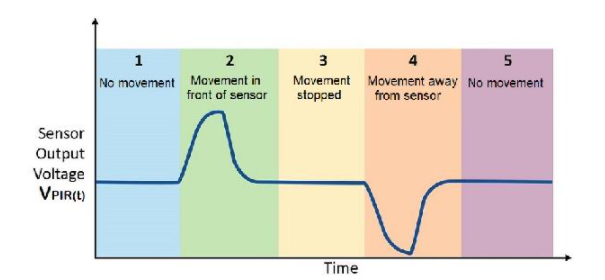
For example, when designing battery-powered sensor nodes for applications such as home security systems, passive infrared (PIR) sensors are usually used inside and outside the residence to detect suspicious movements. The PIR sensor can detect the change in the amount of infrared radiation sensed by the sensor element. This change will vary depending on the temperature and surface characteristics of the object within the detection range of the sensor. When a person passes the detection range of the sensor, the sensor will detect that the ambient temperature has changed to human body temperature, and then return to the ambient temperature. It converts the change in the amount of infrared radiation caused when a person enters into a change in the output voltage (VPIR(t)). For other objects with the same ambient temperature but different surface characteristics, the sensor will also detect different radiation patterns, as shown in Figure 1.

The output signal level of the PIR sensor is usually very low, less than 1 mV. To detect motion while avoiding false detections, the analog signal needs to be amplified first and then sampled by the analog-to-digital converter (ADC). In a typical PIR solution, signal amplification is implemented using a high-gain multi-stage operational amplifier (Op Amp), which will increase the complexity of the design, increase the number of components, reduce power efficiency and increase costs. Please continue reading below to learn how a small and energy-efficient MCU can help reduce these adverse effects.
Design complexity
If the PIR sensor node design is based on a small MCU with the required feature set (such as 12-bit differential ADC and programmable gain amplifier (PGA)), the need for external components can be reduced, and board space and bill of materials (BOM) can be saved. )cost. Therefore, consider using MickroE's PIR click sensor. It is a printed circuit board (PCB) that contains all the passive components required to form a functioning PIR sensor node. The click board is based on an op amp solution, and ADC, resistors and capacitors are included, so it can be used out of the box for easy prototyping and evaluation. To facilitate easy prototyping, a typical setup that can be used is to use the PIR click board with Microchip's Curiosity Nano substrate for Click boards™ and the Curiosity Nano evaluation kit. If MCUs such as Microchip Technology's ATTiny1627 with 12-bit differential ADC and PGA are used, the PIR sensor node solution can gain advantages. Since there is no need to use an external operational amplifier to amplify the signal, the number of external components can be significantly reduced. In addition, there is no need for an external ADC, so many other passive components such as resistors and capacitors can be omitted.
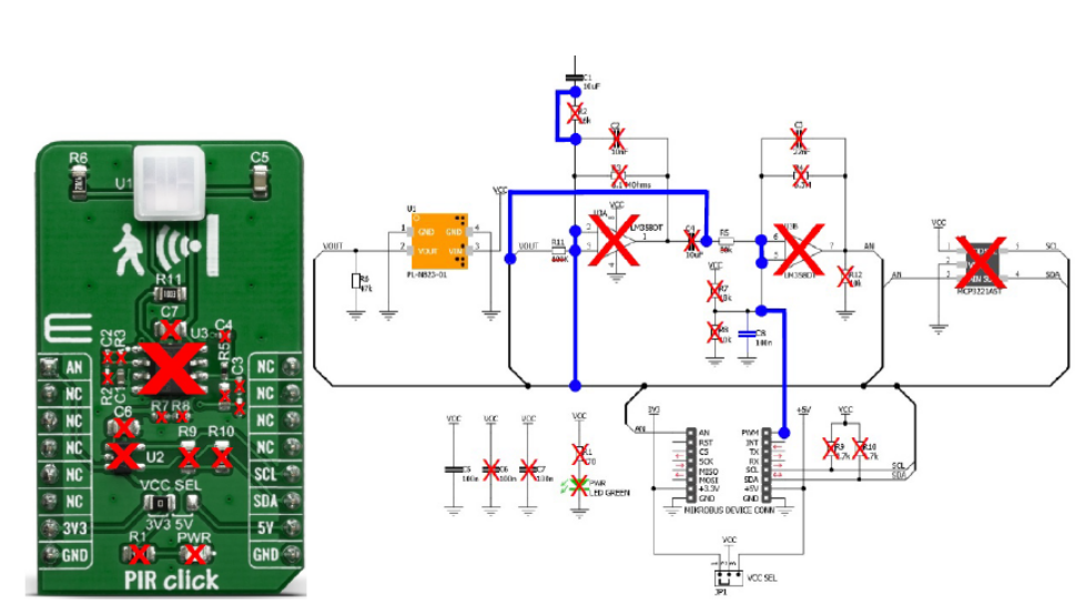
Therefore, the use of this type of MCU can significantly reduce the PCB wiring work of PIR click. Figure 2 shows the components that can be omitted (X) and the new connection method (blue line).
Note: The figure shows an example of modification based on PIR click, because this modification is more convenient than designing a new PCB and obtaining the required components. The modified solution does not conflict with the purpose of the click board.

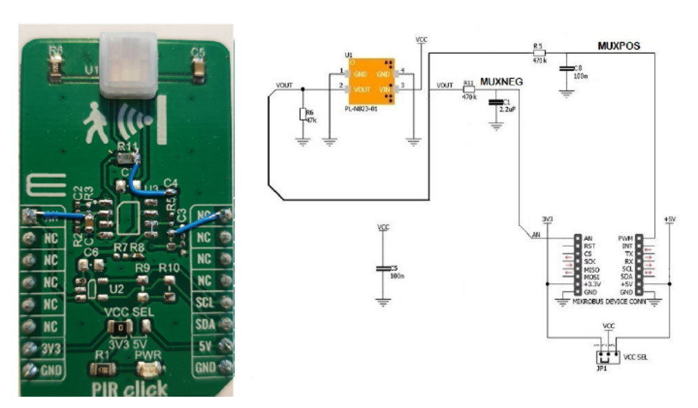
After the above modification, the built-in 12-bit differential ADC and PGA can be used. After selecting a suitable MCU, the required external components can be greatly reduced, as shown in Figure 3.

After reducing the external components used, if the external components need to be replaced, the hardware precautions to be considered are also reduced accordingly, so the hardware and PCB design are cleaner and more compact. In addition, because more tasks are handled in the MCU, the software and firmware are also more compact and efficient. The management of timing and synchronization is also more convenient and concise.
If most of the complexity of sensor node design is transferred from hardware to MCU and central processing unit (CPU) and managed in firmware, you can change and add functions more flexibly during the development process without having to spend time redesigning Circuit board layout, which can save design time and cost. At the same time, code optimization for other factors such as power consumption is also more convenient. By simply changing the parameter settings, designers can change the application code to add functionality, or optimize the code to reduce power consumption or sensitivity related to environmental conditions. When the ambient temperature exceeds 30°C, it may be difficult for the sensor to detect when someone enters the detection range. Optimizing the code can reduce the sensitivity of the system to changes in ambient temperature. When adding functions, you can add machine learning functions to identify movement patterns and help the system learn how to distinguish noise or human and animal movements.
For motion detection applications using PIR sensors, MCUs such as ATTiny1627 have most of the required functions built-in, so the complexity of the design can be transferred from hardware to firmware and software. This reduces complexity while increasing flexibility.
Power Efficiency
For wireless sensor nodes, power consumption is an important consideration. This is because the longer the service life of the battery, the longer the service life of the sensor node, and therefore the longer the service life of the entire sensor network system. This applies to all wireless sensor systems. If tens, hundreds or even thousands of sensors have been installed to implement different monitoring functions, when the node is shut down, the node will be regarded as dead or malfunctioning. For larger sensor systems, replacing the battery or the node itself means additional costs for the end user, and when the node is off, the system will fail or fail to fully function, so it may not be issued in the event of an unexpected event notify. Therefore, the longer the battery life, the better.
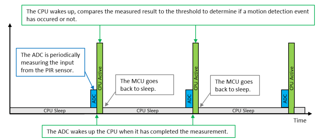
Because the MCU has a sleep mode and can wake up quickly, the power consumption of each sensor node can reach a very low level. The node can sleep. When a temperature change occurs within the detection range of the sensor and movement is detected therefrom, the node will wake up quickly and return to sleep mode after completing the signal processing. Therefore, the working time of each battery-powered node can be extended without the need to replace the battery. See Figure 4 for an understanding of how the CPU operates when using sleep mode and fast wake-up. The power consumption depends on the specific application and will vary according to the configuration, sampling time and filtering parameters of the PIR sensor. These factors also affect the detection range and/or sensitivity of the sensor. If the application needs to achieve lower power consumption, these parameters can be adjusted to further reduce power consumption.

MCUs such as ATTIny1627 are compact and powerful, and have built-in smart and complex features and functions that can improve current consumption and power consumption efficiency, thereby extending the service life of battery-powered networking applications, reducing design complexity, and cutting total system costs. Reduce time to market