June 04, 2019
2973
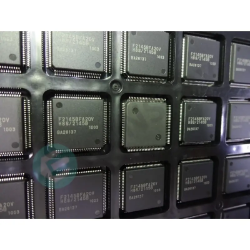
The PCBs of information products are now high-density boards, usually 4-layer boards. As the density increases, the trend of use is a 6-layer board, and its design always needs to consider the balance of performance and area. On the one hand, there can be more space for components, and the wider the line width and the line spacing, the benefits for EMI, audio, ESD and other aspects of performance. On the other hand, the compactness of digital product design is also a trend and need. Therefore, you need to find a balance point when designing. As far as the ESD problem is concerned, there are many places to pay attention to in the design, especially regarding the design and line spacing of the GND wiring. In some products, there is a big problem with ESD, and there is no reason. Through repeated research and experiments, it is found to be a problem in PCB design. Here is a summary of the points that should be noted in PCB design:
(1) The distance between the edge of the PCB (including the boundary of the via) and other wirings shall be greater than 0.3 mm;
(2) The board edges of the PCB are preferably all surrounded by GND traces;
(3) The distance between GND and other wiring is kept between 0.2-0.3mm;
(4) The distance between the Vcc pin and other wiring is kept between 0.2-0.3mm;
(5) The distance between important lines such as Reset, Clock, etc. and other wirings should be greater than 0.3mm;
(6) The distance between the high-power line and other wiring is kept between 0.2-0.3mm;
(7) There should be as many vias (Via) as possible between the GNDs of different layers;
(8) Avoid sharp corners in the final paving, and sharp corners should be as smooth as possible.