September 17, 2020
2971
The phase-locked loop (PLL) circuit is a feedback system composed of a voltage controlled oscillator (VCO) and a phase detector. The oscillator signal tracks whether the applied frequency or phase modulation signal has the correct frequency and phase. When you need to generate a stable high output frequency from a fixed low-frequency signal, or when you need to change the frequency quickly, you can use PLL. Typical applications include the use of high-frequency, telecommunications and measurement technologies to achieve filtering, modulation and demodulation, and to achieve frequency synthesis.

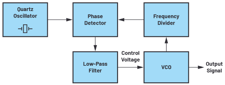
Figure 1. Block diagram of phase-locked loop
Figure 1 shows a block diagram of a PLL-based frequency synthesizer. The VCO generates an output signal. Keep it at the set frequency by PLL and lock to the reference frequency. The reference frequency is usually provided by a very precise quartz oscillator. In the feedback path part of the phase-locked loop circuit, an adjustable VCO frequency division ratio is provided through a frequency divider before the phase detector.
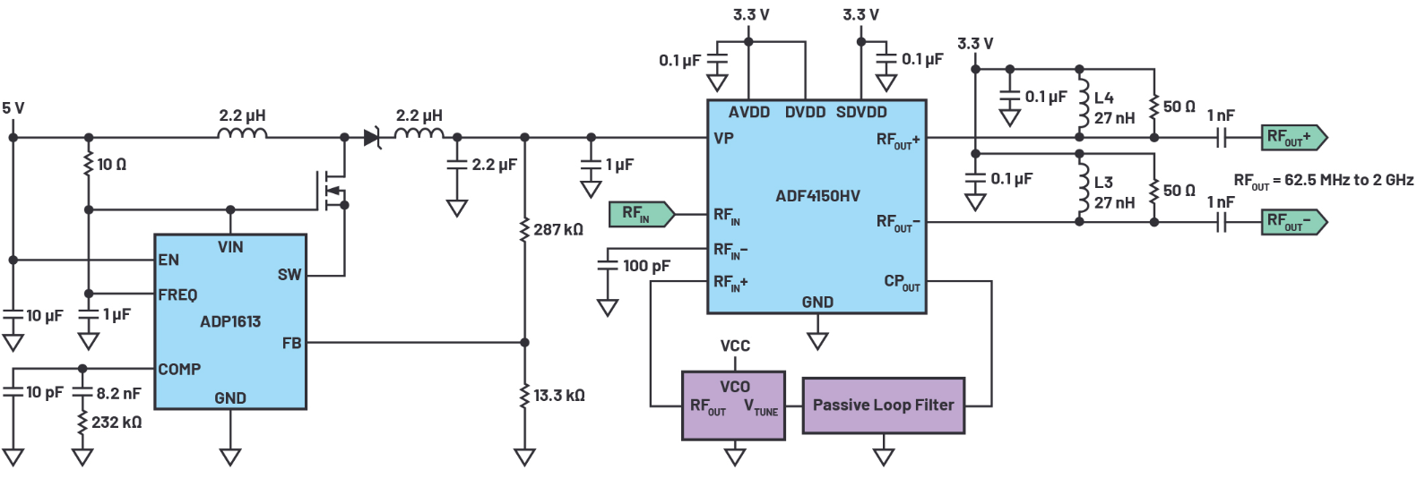
The VCO contains adjustable tuning elements, such as varactor diodes whose capacitance changes with the input voltage. Therefore, the PLL circuit can be regarded as a VCO feedback control system. The input or control voltage required by the VCO is usually higher than the power supply voltage provided to the PLL circuit. The power supply voltage is generally 3.3 V or 5 V, and the VCO may require a voltage higher than 20 V depending on frequency requirements. To generate a wider range of frequencies, a VCO with a wider tuning range can be used. Figure 2 shows an example of a simple circuit that supports a VCO in the gigahertz range.
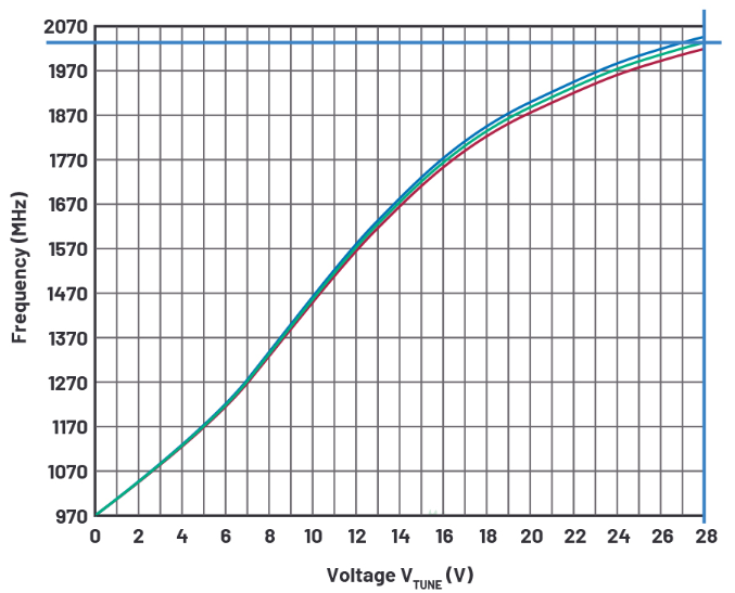
The VCO can use DCYS100200-12 from Synergy Microwave Corporation. This product generates 2 GHz frequency at 28 V (VTUNE), as shown in Figure 3.
There are several possible options for generating high control voltages. One is to use an active loop filter, which is basically composed of a high-speed amplifier and a low-pass filter, which can convert the output pulse from the phase detector (CPOUT) into a clean DC voltage. Alternatively, you can use a PLL frequency synthesizer with an integrated charge pump, such as ADI's ADF4150HV, which does not require an additional active loop filter. Although both solutions require high-voltage power supplies, using the ADF4150HV can reduce the number of components required. It can also avoid distortion and phase noise caused by active filter amplifiers. In addition, the ADF4150HV allows the realization of a fractional-N or integer-N phase-locked loop frequency synthesizer. The final VCO frequency can be divided by 1, 2, 4, 8, or 16, so that the output frequency can reach as low as 31.25 MHz.

Figure 2. Simplified circuit for high-voltage charge pump power supply for ADF4150HV.

Figure 3. DCYS100200-12 control voltage and frequency relationship curve 1
The high voltage required by the integrated charge pump of the ADF4150HV can be generated using the ADP1613 DC-DC boost converter without degrading PLL performance. The ADP1613 is a high-efficiency switching regulator with integrated power transistors that can easily achieve output voltages up to 20 V. It is also possible to use additional external components to achieve higher output voltages, especially through external power transistors. The switching frequency of the ADP1613 can be adjusted from 650 kHz to 1.3 MHz. This can achieve better transient response and simple noise filtering. Generally speaking, it is recommended to select a switching frequency higher than 1 MHz to reduce the switching noise through the PLL loop filter.
The phase-locked loop frequency synthesizer circuit using ADF4150HV provides ultra-wideband PLL function by using an integrated RF divider. The operating frequency range is 62.5 MHz to 2 Ghz. By using the same PLL hardware design, different frequencies can be generated for multiple different hardware platforms in the system. However, if a design is required to be applicable to different VCO types, the corresponding loop filter needs to be integrated in the design. In this way, the reliable operation of the phase-locked loop can be ensured. In order to achieve a relatively wide output frequency adjustment range, and related higher output power, each RF output of the ADF4150HV also requires a small filter. Connecting a 27 nH inductor and a 50 Ω resistor in parallel can effectively adjust frequencies up to 3 GHz. This resistor provides a defined output impedance. The lower inductance will cause the frequency band to extend to a lower range.
Nowadays, it is also possible to provide all-in-one integrated solutions suitable for a larger frequency range (that is, suitable for PLLs, filters, and VCOs), but due to the close distance between different components, it may lead to useless coupling. The discrete design and the physical separation achieved thereby can sufficiently reduce this risk.
The PLL frequency synthesizer simulation tool ADIsimPLL™ can also provide effective assistance for the development of HF function modules and the modeling of HF signal chain devices. By using this tool, it is easier for designers to simulate all important non-linear effects that will affect PLL performance; for example, unwanted spurs (spurious frequencies) that appear during frequency synthesis.