August 20, 2020
2886
Current ferroelectric tunnel junctions are based on two types of ferroelectric materials, perovskite-type ferroelectrics (such as BaTiO3 and PbZr0.2Ti0.8O3) and oxide-type ferroelectrics (such as HfO2 and Hf0.5Zr0.5O2). These two types of ferroelectric materials have their own advantages and disadvantages for ferroelectric tunnel junctions. The ferroelectric tunnel junction based on perovskite-type ferroelectrics can achieve a higher tunnel resistance (about 106) when using a metal/ferroelectric/semiconductor sandwich structure, but because this ferroelectric material must be grown in a special On the substrate, it is difficult to be compatible with traditional silicon processes, which greatly affects the application prospects. Ferroelectric tunnel junctions based on oxide ferroelectrics have silicon process compatibility. However, due to the nature of the material and the limitation of the regulation mechanism, the current tunneling resistance has not been able to break through 100, and there is still a large distance from practical application. In addition, the barrier height adjustment in these ferroelectric tunnel junctions is very limited (about 0.1 eV), which limits the improvement of its performance. In recent years, with the discovery of two-dimensional room temperature ferroelectrics such as CuInP2S6 (CIPS) and In2Se3, ferroelectric tunnel junctions have taken on another new development direction. Recently, the Han Wang team at the University of Southern California (https://hanw.usc.edu/) achieved a tunneling resistance of up to 107 in the graphene/CIPS/Cr two-dimensional van der Waals ferroelectric tunnel junction, and at the same time benefited from the single Layer graphene has a very small density of states near the Dirac point, and they have observed a barrier height adjustment of up to 1 eV in this type of van der Waals ferroelectric tunnel junction. The ferroelectric tunnel junction takes into account both silicon process compatibility and high tunneling resistance, and is expected to become a commercial high-performance ferroelectric memory in the future. The related results were published on Nature Electronics on July 6, 2020 under the title of "High tunnelling electroresistance in a ferroelectric van der Waals heterojunction via giant barrier height modulation". Jiangbin Wu and Hung-Yu Chen from the University of Southern California are the co-first authors. Professor Han Wang, Professor Jing Guo from the University of Florida and Professor Qibin Sun from the University of Science and Technology of China are the co-corresponding authors of this article. This work was assisted by Professor Xi Ling of Boston University and Professor Fanxin Liu of Zhejiang Sci-Tech University.

In the experiment, the researchers first made a single-layer graphene, CIPS and Cr into a vertical heterojunction device. The room temperature ferroelectricity of CIPS was verified by piezoelectric force microscope and capacitor voltage response. Through voltage pulses in different directions, the polarization direction of CIPS can be reversed to obtain a tunnel resistance of up to 107 (Figure 1). The current and voltage characteristics of the device are well described by the simulation based on the unbalanced Green's function. Such high tunneling resistance comes from the small density of states near the Dirac point of graphene and the unique interface properties of van der Waals heterojunctions. When the iron polarization direction in CIPS faces graphene, graphene is n-type doped, and the barrier is very low at this time, and the tunnel junction is in an open state. When the iron polarization direction in CIPS faces Cr, the graphene is p-type doped, and the barrier is high at this time, and the tunnel junction is in the off state. Because of the small density of states near the Dirac point, the Fermi level of graphene changes greatly when the ferroelectric polarization is reversed, that is, the barrier height changes greatly, resulting in a large tunnel resistance. Using Raman spectroscopy and Kelvin force microscopy, the researchers detected barrier height differences as high as 1 eV (Figure 2).
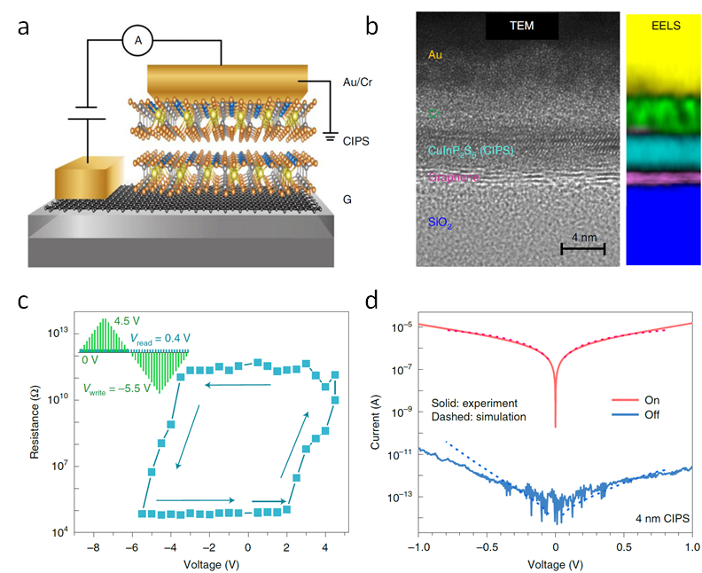
Figure 1. (a) Schematic diagram of the van der Waals ferroelectric tunnel junction. (b) TEM and EELS images of the junction section of van der Waals ferroelectric tunnel. (c) The switching characteristics of the Van der Waals ferroelectric tunnel. (d) Current and voltage characteristics of van der Waals ferroelectric tunnel junction on and off. In order to verify the role of graphene in this type of van der Waals ferroelectric tunnel junction, the researchers also compared the difference in tunnel resistance between the graphene/CIPS/Cr ferroelectric tunnel junction and the Au/CIPS/Cr ferroelectric tunnel junction. The tunneling resistance in the Au/CIPS/Cr ferroelectric tunnel junction without graphene is about 50, which is much lower than the 107 in the van der Waals ferroelectric tunnel junction. In addition, as the thickness of the graphene increases, the tunnel resistance of the van der Waals ferroelectric tunnel junction also gradually decreases, which fully reflects the advantage of single-layer graphene used for tunnel barrier height adjustment. They also verified that this type of van der Waals ferroelectric tunnel junction has the characteristics of high-speed read and write and high read and write durability, as well as its long-lasting data retention capability, making it an ideal choice for the next generation of high-performance non-volatile memory.
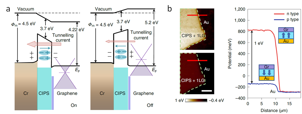
Figure 2. (a) Schematic diagram of the band structure of van der Waals ferroelectric tunnel junction. (b) Fermi level adjustment of graphene in van der Waals ferroelectric tunnel junction detected by Kelvin force microscope.