August 24, 2021
2141
What craft edge?
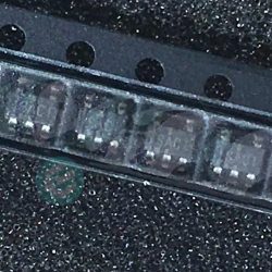
Although the craft edge is not the real element that constitutes a printed circuit board (PCB), it plays a very important role for a PCB assembled by surface mount technology (SMT). As the name suggests, the function of the craft side is the same as the railway. A conveyor belt is used to transfer the PCB during the SMT assembly process for solder paste printing, pick and place, reflow/wave soldering and inspection. Unless the circuit board is accurately pasted to the conveyor belt through the process edge, the circuit board will never be transferred safely and effectively. Figure 1 below shows the structure of the process side.
Why do we need craft edges?
The main responsibility of the process side lies in its role as an "assisted" manufacturing, even if the manufacturability of the assembly is smoothly proceeded. This stems from the need for SMT placement machine rails to firmly fix the side of the circuit board and transfer it to the reflow oven. Therefore, if the design of the component is too close to the edge of the board, it may be "attacked" when picking, placing or soldering the component, resulting in errors or even failure. In addition to SMT assembly, this situation also applies to through-hole component assembly and wave soldering.
Why does PCB require the use of craft edges?
Although process edges are of great significance to PCB assembly, not all PCBs must rely on process edges during assembly. After all, the production of process edges leads to an increase in total cost. So, which type of PCB needs crafting edge?
Generally speaking, two factors play a leading role in determining whether a process side is needed. Once any one of the conditions is met, the technical requirements must be carefully considered:
1. The distance between the component position and the edge of the circuit board. If the distance between the component and the edge of the circuit board is designed to be less than 3mm, the distance between the component and the edge of the PCB is so close that errors or malfunctions may occur. The process edge is needed to expand the distance between the component location and the conveyor belt where the equipment is installed.
2. Reference mark. When there is no fiducial mark on the PCB, it is necessary to use the craft edge where the fiducial mark needs to be accurately implanted to ensure the correct coordinates so that the component position fully meets the requirements specified in the design document.
What should be considered on the side of the craft?
1. The width of the craft edge. Generally speaking, according to specific assembly requirements and assembly equipment parameter requirements, the width of the process side is in the range of 1.5mm to 5mm. Therefore, it is very necessary to consult the contract assembler to ensure that your design is compatible with the corresponding assembly equipment.
2. The cost of the process side. With the manufacturing of process edges, material consumption will definitely increase, so the total cost will also increase. How to balance PCB cost and manufacturability can be considered as the primary consideration for PCB design engineers and PCB manufacturers or assemblers. In order to minimize the cost, the usual method is to minimize the application of the process side by designing the best layout for the PCB panel, which can minimize the application of the process side. Reliable PCB manufacturers or assemblers have sufficient knowledge and experience to provide customers with ideal solutions based on quality and cost considerations.
How to remove the craft edge?
Since the process edge is not part of the mechanical system of the circuit board, it is no longer useful after the PCB is manufactured or assembled, and you should consider removing it from those boards. Currently, there are three ways to delete the craft edge:
1. Routing sub-board machine. In terms of quality alone, it is the most effective choice. The machine mainly relies on a milling cutter, which can separate the panel PCBA into independent parts in a high-speed rotation according to a programmed route. Compared with the V-cutting and splicing machine, it has obvious advantages, that is, the V-cutting and splicing machine can only cut the panel along a straight line, which is far beyond it. In addition, this will result in a clean and tidy board edge, while V-cutting de-stamping machines or manual de-stamping will usually cause blurring. Therefore, it helps to improve quality and reduce waste, but it is expensive due to the complicated operation process and low flexibility.
2. V-shaped cutting and jigsaw machine. It can perform cutting operations in a straight line along the V-groove, and the cost of blade consumables is relatively high. However, the total cost is lower than the routing tool splitter.
3. Manually divide the board. It relies on hands or needle-nose pliers for separation, and has the advantages of convenient operation and low cost. However, greater mechanical stress may be generated, so that components near the edge of the board may break down.