March 01, 2019
3340
In the case of IIC communication, there are generally two operations of writing and reading. We use AT24C02 to explain specifically.
AT24C02 chip works
The AT24C02 chip is an EEPROM device with an IIC interface. The so-called EEPROM is an electrically erasable programmable read only memory, which is a kind of ROM. It is a read-only memory, that is, power-down can continue to store data, while at the same time can be erased and rewritten under the action of ordinary voltage, which greatly facilitates the development of the single-chip microcomputer, and now many ROMs on the computer Is the EEPROM used.
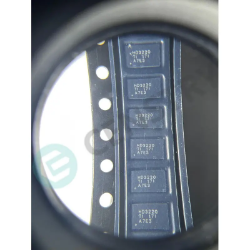
The pin diagram of the AT24C02 is as follows:
A0, A1, A2 are used to define the chip address (described later), VCC and GND are the positive and negative interfaces of the power supply, SCL and SDA are the data bus of IIC, and WP is the write protection (if connected to VCC, all contents of the chip are It is protected, can only be read and can not be written, generally we are directly grounded).
The slave address of the AT24C02 is shown in the following table. The first four digits of 1010 are fixed values. A0, A1, and A2 correspond to the 1, 2, and 3 lead angles of the chip. The last digit indicates read (1) or write (0). .
Implementation:
The AT24C02 has 2Kbit (256byte) memory divided into 32 pages, and its write operations include byte write and page write.
Byte write is to write to the byte of the specified address, the timing is:
1 send start signal
2 Transmit slave address + write flag "0" and wait for the reply signal
3 send the address to be written, and wait for the response signal
4 send the data to be written, and wait for the response signal
5 Send a stop signal.
(Note that the slave address is distinguished from the address in 4. The slave address is used to distinguish the slave on the bus, and this address is the internal address of the device and is used for storage.)
The page write is based on the byte write. Before step 5, the fourth step is used multiple times. That is, the stop signal is not sent at the end, but the data is continuously sent. At this time, the AT24C02 will automatically increment the address. All data is sent and the stop signal is sent.
The read operation of 24C02 has current address read, random read and sequential read.
Random reads can specify the address of the data to be read, the specific timing:
1 send start signal
2 Transmit slave address + write flag "0" and wait for a response
3 send the address of the data to be read, and wait for the response
4 resend a start signal (also known as the restart signal)
5 Transmit slave address + read flag "1" and wait for a response
6 Receive the incoming data, send a non-acknowledgement signal after receiving the data
7 sends a stop signal.
(Note that the slave address is distinguished from the address in 4. The slave address is used to distinguish the slave on the bus, and this address is the internal address of the device and is used for storage.)
The current address read is only the address of the last operation of the chip and the data of one location (mainly used when the last operation address is known). The specific timing:
1 send start signal
2 Transmit slave address + read flag "1" and wait for a response
3 Receive the incoming data and then send a non-acknowledgement signal
4 send a stop signal.
The sequential read is based on the first two read operations, after receiving the data, the response signal is sent, and then you can continue to read the last operation address plus one data (this is implemented inside the chip), when reading After the data is enough, a non-acknowledgement signal is sent, and finally a stop signal is sent.
Knowing this, you can read and write on the AT24C02.
The basic circuit diagram is as follows: