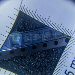
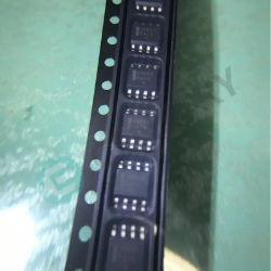
Power Switch/Driver 1:1 N-Channel 4A 8-WSON (2x2)


Images are for reference only.
See Product Specifications for product details.
Power Switch/Driver 1:1 N-Channel 4A 8-WSON (2x2)
Orders over $200 are eligible for a limited edition Chinese-style gift.
Orders over $1000 qualify for a $30 shipping fee waiver.
Orders surpassing $5000 enjoy waived shipping and transaction fees.
These offers are applicable to both new and existing customers and are valid from January 1st, 2024, to December 31st, 2024.
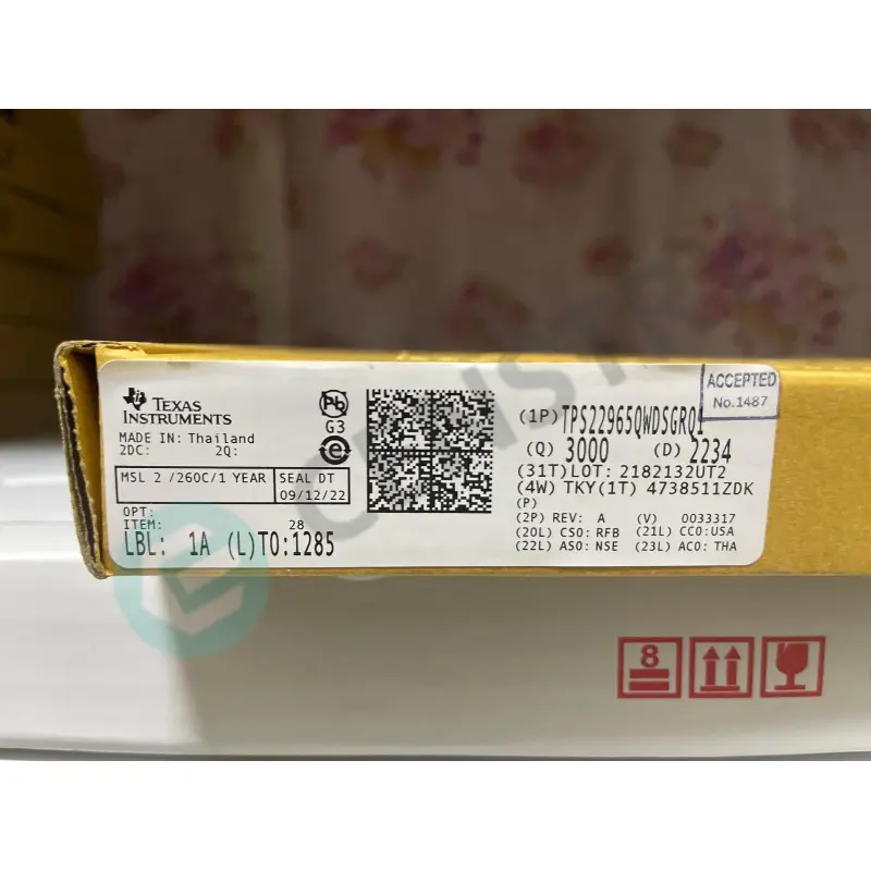
TI
TPS22965QWDSGRQ1 datasheet
WSON-8
RF Integrated Circuits
 Lead free/RoHS Compliant
Submit your quote request now, and we expect to provide a quote within July 27, 2024. Place your order now, and we expect to complete the transaction within July 31, 2024. Ps:Time is according to GMT+8:00.


1 Features
• Qualified for automotive applications
– AEC-Q100 qualified
– Device temperature grade 2: –40°C to +105°C
(TPS22965-Q1, TPS22965N-Q1)
– Device temperature grade 1: –40°C to +125°C
(TPS22965W-Q1, TPS22965NW-Q1)
– Device HBM ESD classification level 3A
– Device CDM ESD classification level C6
• Functional Safety-Capable
– Documentation available to aid functional safety system design
• Integrated single channel load switch
• Input voltage range: 0.8 V to 5.5 V
• Ultra-low on resistance (RON)
– RON = 16 mΩ at VIN = 5 V (VBIAS = 5 V)
– RON = 16 mΩ at VIN = 3.6 V (VBIAS = 5 V)
– RON = 16 mΩ at VIN = 1.8 V (VBIAS = 5 V)
• 4-A maximum continuous switch current
• Low quiescent current (50 µA)
• Low control input threshold enables use of 1.2-, 1.8-, 2.5- and 3.3-V logic
• Configurable rise time
• Quick Output Discharge (QOD) (TPS22965-Q1 and TPS22965W-Q1 only)
• WSON 8-pin package with thermal pad
2 Applications
• Automotive electronics
• Infotainment
• ADAS (Advanced Driver Assistance Systems)
3 Description
The TPS22965x-Q1 is a small, ultra-low-RON, singlechannel load switch with controlled turn-on. The device contains an N-channel MOSFET that can operate over an input voltage range of 0.8 V to 5.5 V and can support a maximum continuous current of 4 A. The VOUT rise time is configurable so that
inrush current can be reduced. The TPS22965-Q1 and TPS22965W-Q1 devices include a 225-Ω on-chip
load resistor for quick output discharge when the switch is turned off.
The TPS22965x-Q1 devices are available in a small, space-saving 2-mm × 2-mm 8-pin WSON package (DSG0008A) with integrated thermal pad allowing for high power dissipation. The TPS22965-Q1 and TPS22965N-Q1 devices are characterized for operation over the free-air temperature range of –40°C to 105°C. Furthermore, the TPS22965WQ1 and TPS22965NW-Q1 devices feature wettable flanks in the same WSON package (DSG0008B) and it is characterized for operation over the free-air temperature range of –40°C to +125°C.

Request a quote TPS22965QWDSGRQ1 at censtry.com. All items are new and original with 365 days warranty! The excellent quality
and guaranteed services of TPS22965QWDSGRQ1 in stock for sale, check stock quantity and pricing,
view product specifications, and order contact us:[email protected].
The price and lead time for TPS22965QWDSGRQ1 depending on the quantity required, please send your request to us,
our sales team will provide you price and delivery within 24 hours, we sincerely look forward to cooperating with you.

ON
3504 PCS
NCP1654BD65R2G .PDF
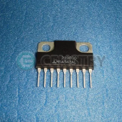
MITSUBISHI
200 PCS
M54543AL .PDF
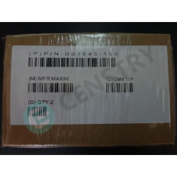
DALLAS
400 PCS
DS1643-150 .PDF
NEXPERIA
3500 PCS
HEF4094BT .PDF
2024-07-26
Honest Broker, Thank You
2024-07-26
Its always a pleasure working with you.
2024-07-26
Karin is very nice to work with. Active and fast reply. Hope we have more chance to do business.
2024-07-26
Censtry elec is a very faithful and understanding client. They make shipment in time. I like working with them.Looking forward to more business chances soon.
2024-07-25
Multiple orders with this company. Always deliver quality product and quick shipments. We hope to do a lot more business in the future.
2024-07-24
One of the best vendors in Asia. Period.
2024-07-21
Peter is well and make a fast shipping . It is a good company!
2024-07-16
professional!!!!
2024-07-05
received good quality products in time...
2024-06-14
Sam and Sunny are professional and great to deal with!

We highly value your feedback. Please share your most genuine review.
*Kindly log in to your account before posting a comment