Published :8/26/2020 3:19:48 AM
Click Count:2103
1 billion 7nm chips are shipped, 5nm mass production, and N5+, N4, and N3 mass production are in preparation.
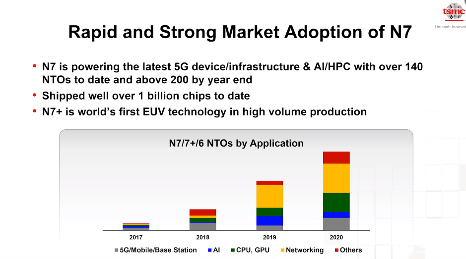
In July of this year, TSMC announced the use of a 7nm process to produce the billionth chip for the latest 5G equipment and infrastructure
Construction and AI and HPC applications. In addition, TSMC is also the first wafer manufacturing service company to use EUV technology for commercial production of the 7-nanometer generation. TSMC's 7nm process officially entered mass production in April 2018, and has manufactured chips for more than 100 products from dozens of customers.
Since the beginning of this year, in the fight against the COVID-19 epidemic, technology has been used in fields such as temperature sensors, self-driving delivery vehicles, and robots. It also needs computing power to help researchers study diseases and find treatments. In addition, the use of the Internet has seen a significant jump this year.
TSMC CEO Wei Zhejia said that TSMC is firmly optimistic about 5G deployment and AI generalization. It is expected that these two major trends will continue for a long time, and TSMC will collaborate with our ecosystem partners in the process and support our client.
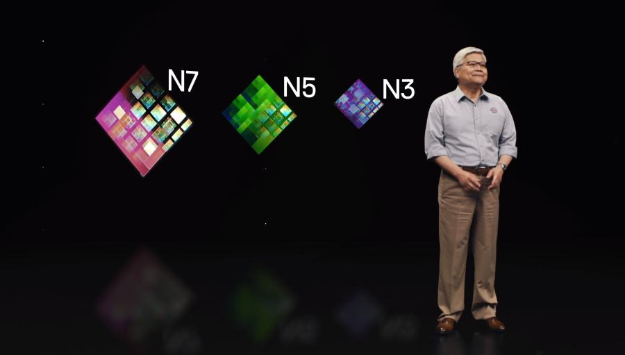
In terms of 7nm, N7 and N7+ have been mass-produced, and continue to maintain high yields, maintaining high speed and logic density.
N5 and N5+, the latter will be mass-produced in 2021
N5 has also been mass-produced. TSMC’s N5 is the most advanced process technology in the industry and provides the best PPA. Compared with N7, N5 has a 15% increase in speed, a 30% reduction in power consumption, and an 80% increase in logic density. The extensive use of EUV technology in the N5 process demonstrates TSMC's leading position in advanced manufacturing.
TSMC plans to launch an enhanced version of N5 N5P in 2021. Compared with N5, it will bring 5% additional speed increase and 10% power increase.
N4: Trial production is expected in the fourth quarter of 2021 and mass production in 2022
N4 is the newest member of the 5-nanometer process family. It is directly transferred from N5 through fully compatible design rules to provide higher performance, power and density. This will enable customers to take advantage of the fully developed N5 design infrastructure and benefit from the extremely competitive cost/efficiency advantages of N5.
N4 is expected to start trial production in the fourth quarter of 2021, with the goal of mass production in 2022.
TSMC said it believes that the 5-nanometer process family will become another large-scale and long-lasting process of the company.
N3: Trial production is expected in 2021 and mass production in the second half of 2022.
N3 is positioned to become the world's most advanced professional integrated circuit manufacturing service process technology. Its logic density will be increased by 70%, performance will be increased by 15%, and power consumption will be 30% lower than N5.
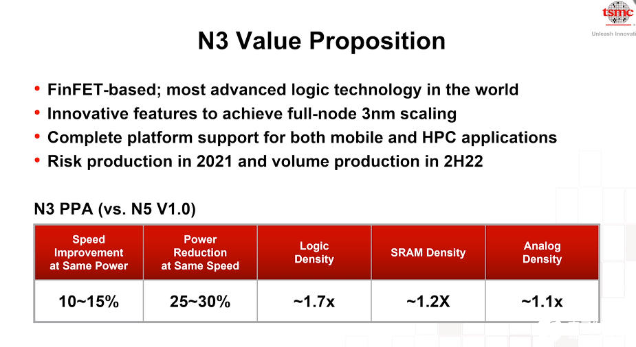
The N3 process will continue to use the FinFET transistor architecture. TSMC executives said there are two important considerations. One is that the R&D team has discovered a new way to increase the performance of FinFET to a new level. The second is to provide the best technology maturity, efficiency and cost, and have a complete platform support action and HPC application, which can bring such innovations to customers as soon as possible.
The trial production of N3 is expected to start in 2021, and the target time for mass production is the second half of 2022.
TSMC will continue the research and development of advanced technology, and is currently working closely with customers to define the technology and specifications of the next important node after N3.
And TSMC executives also introduced that they are studying new materials and breakthroughs in architecture, such as high mobility channels, nanosheets/nanowires, 2D materials, carbon nanotubes, and so on.
Advanced process capacity and expansion: 3nm production base, 2nm R&D center
Since the introduction of the 7nm process for mass production in 2018, TSMC’s 7nm production capacity has gradually increased. It is expected that the 7nm production capacity in 2020 will be more than 3.5 times that of 2018. In 2020, another important process 5nm mass production, a large number of EUV processes will be used to further improve the chip Efficiency and lower power consumption, 5nm production capacity is expected to grow more than 3 times in two years.
From the perspective of global EUV installed capacity, TSMC accounted for 50%, and EUV Wafer Move, TSMC accounted for 60%. The more EUV Wafer Move represents the accumulation of more learning and experience, and it is also one of the indicators of EUV's successful mass production.
In order to meet the market's demand for advanced semiconductor process technology, TSMC's 2020 capital expenditure plan has increased by US$1 billion to between US$16 billion and US$17 billion.
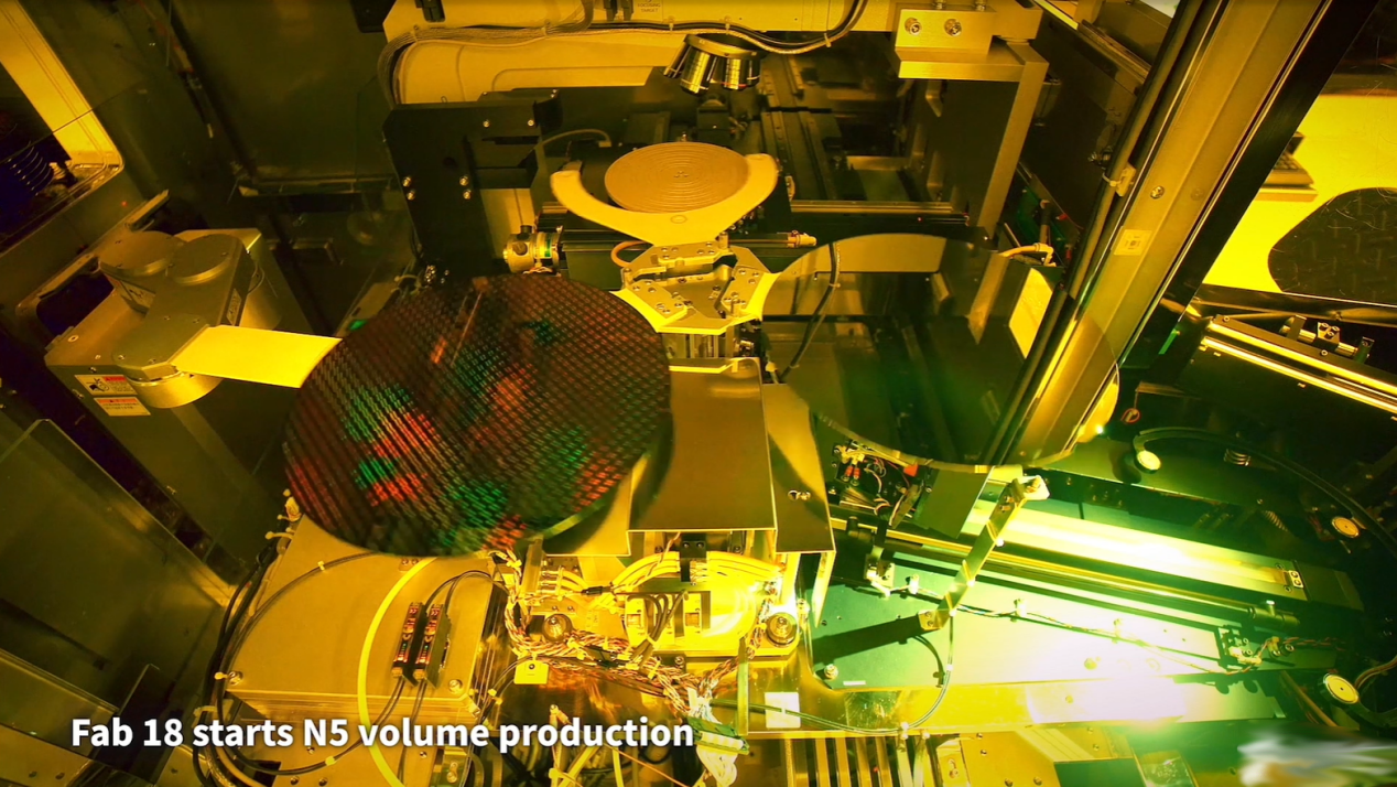
In the TSMC Nanke plant, the first to third phases of the fab 18 are 5nm production bases, of which the first and second phases have begun mass production, and the third phase has begun to install. The fourth to sixth phases of Fab 18 will be the future 3nm production base, which is currently under construction.
The eighth phase of Fab 14 will serve as a production base for special process technologies, and AP2C above Phase 7 of Fab 14 will be a production base for advanced packaging technologies in the future.
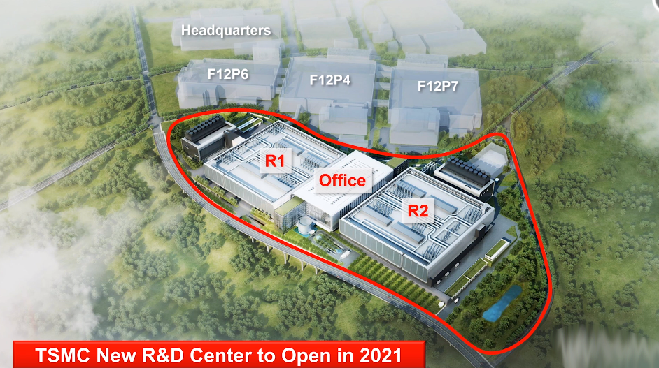
At TSMC’s Hsinchu plant, R1 has begun to build a new R&D center, which is scheduled to be completed in 2021, which will serve as a R&D base for 2nm and more advanced technologies. The nearby fab will be used as a 2nm production base in the future, and land acquisition is currently in progress.
Introduced ultra-low power consumption process technology N12e, integrated 3D IC platform as "3D Fabric"
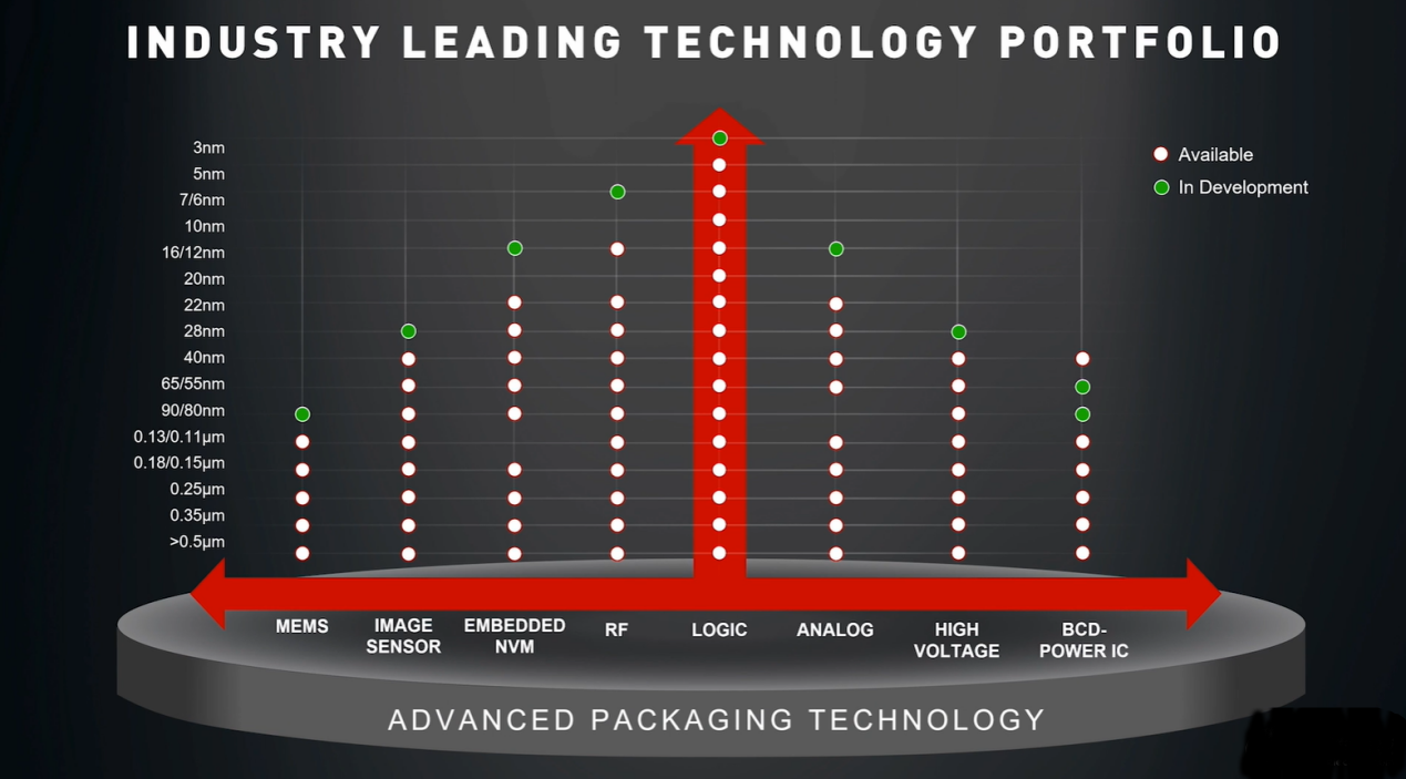
TSMC provides the most extensive special process product portfolio, including MEMS, image sensors, embedded memory, radio frequency, analog, analog, high voltage and power ICs, which can seamlessly integrate with TSMC’s advanced logic processes to provide customers with the best system Level solution.
According to reports, the proportion of TSMC's special process capacity in the company's total production capacity has been increasing year by year, from 38% in 2015 and 54% this year. The total production capacity of special processes this year will grow 10% over last year.
In response to the needs of the Internet of Things and artificial intelligence, TSMC has launched the most advanced ultra-low-power process technology, N12e, which is optimized for edge AI devices.
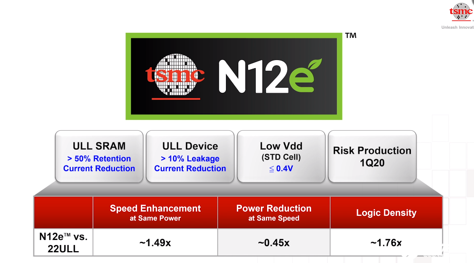
According to reports, N12e is built on the basis of 12FFC + process technology and can reuse the existing IP ecosystem. This is the first ultra-low power process technology using FinFET transistors, which can significantly improve speed, power consumption and logic density. It can also support ultra-low leakage devices and ultra-low Vdd designs as low as 0.4V, which is also a major technological breakthrough for the industry, enabling the most advanced artificial intelligence in the field of Internet of Things (AIoT), mobile and other edge applications Innovation.
In addition, at this technical forum, TSMC announced the integration of 3D silicon stacks and advanced packaging technology families, namely SoIC, InFO, CoWoS and other 3D IC platforms named 3D Fabric. In a situation where 2D scaling is no longer sufficient to integrate system scaling, TSMC’s 3D IC technology can reduce area, improve performance, and integrate different functional requirements. TSMC already has the most advanced wafer-level 3D IC technology in the industry. TSMC will continue to provide the industry's most complete and most versatile internal interconnection solutions for integrating logic chips, high-bandwidth memory and special process chips to realize many innovative product designs.

Wei Zhejia also said that the trust relationship established between TSMC's business model and customers is the key to TSMC's success. He said that we have established a trusting relationship with customers for 33 years. Customer trust has always been our core value and mission, and it is also an integral part of TSMC's business model. The most important thing is that we absolutely do not compete with customers and never launch our own products, so we can invest all resources and focus on ensuring the success of our customers. We will also put in more power to innovate together and contribute to the world together!