Published :12/28/2020 3:37:41 AM
Click Count:2103
my country's first new-generation large-size integrated circuit monocrystalline silicon growth equipment achieved a successful trial production in Xi'an. This is jointly developed by Xi'an University of Technology and Xi'an Eswell Equipment Technology Co., Ltd. The length of the monocrystalline silicon rod manufactured this time is 2.1 meters and the diameter is 300mm, which is 12 inches, which marks a breakthrough in the key technology of 12-inch silicon wafers in the field of chip manufacturing in my country and solves the problem of "stuck neck".

According to the Science and Technology Daily, the research and development of the project is led by the team of Professor Liu Ding from Xi'an University of Technology. Professor Liu Ding has worked intensively in the field of semiconductor silicon single crystal growth for many years. He has presided over a number of major national science and technology projects and key projects of the National Natural Science Foundation. In recent years, he has made technological breakthroughs and obtained a number of landmark results.
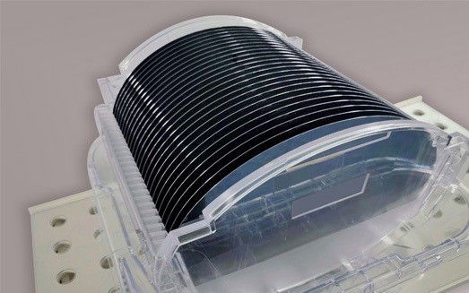
According to Eswell’s introduction, the production of silicon single crystal rods first requires putting high-purity polysilicon into a quartz crucible, heating it to above 1400°C, and melting it into a silicon solution, and then immersing the seed crystal into the silicon melt, seeding and setting the shoulders. , Shoulder turning, equal diameter growth, finishing and other steps to complete the drawing of a single crystal silicon rod. After the monocrystalline silicon rod is produced, the ingot is cut into silicon blocks with a length of 300-400 mm, and then a sheet with a thickness of about 1 mm is obtained by wire cutting, which is then polished and cleaned to obtain a high-quality polished sheet .
Xi'an Eswell Silicon Wafer Technology Co., Ltd. is a domestic large-scale monocrystalline silicon manufacturing backbone enterprise. Since 2018, it has cooperated with the team of Professor Liu Ding of Xi'an University of Technology. The company is able to manufacture 12-inch silicon wafers with no dislocations, no native defects, ultra-flat and excellent nano-topography for the production of integrated circuit chips below 28nm. In addition, the company also provides wafer processing, cleaning and epitaxy services.
At present, Eswell has a silicon industrial base in Xi'an, which will be constructed in two phases, with a designed production capacity of 500,000 pieces per month in the first phase. The successful production of this large-scale monocrystalline silicon growth equipment will help meet the urgent needs of my country in the development of integrated circuits and get rid of the situation of being restricted by others.