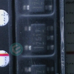
IC GATE DRVR LOW-SIDE SOT23-5


Images are for reference only.
See Product Specifications for product details.
IC GATE DRVR LOW-SIDE SOT23-5
Orders over $200 are eligible for a limited edition Chinese-style gift.
Orders over $1000 qualify for a $30 shipping fee waiver.
Orders surpassing $5000 enjoy waived shipping and transaction fees.
These offers are applicable to both new and existing customers and are valid from January 1st, 2024, to December 31st, 2024.
TI
UCC27517DBVR datasheet
SOT23-5
IC Chips
 Lead free/RoHS Compliant
Submit your quote request now, and we expect to provide a quote within April 26, 2024. Place your order now, and we expect to complete the transaction within May 01, 2024. Ps:Time is according to GMT+8:00.


1 FEATURES
• Low-Cost, Gate-Driver Device Offering Superior Replacement of NPN and PNP Discrete Solutions
• 4-A Peak Source and 4-A Peak Sink Symmetrical Drive
• Fast Propagation Delays (13-ns typical)
• Fast Rise and Fall Times (9-ns and 7-ns typical)
• 4.5-V to 18-V Single Supply Range
• Outputs Held Low During VDD UVLO (ensures glitch free operation at power-up and power-down)
• TTL and CMOS Compatible Input Logic Threshold (independent of supply voltage)
• Hysteretic Logic Thresholds for High Noise Immunity
• Dual Input Design (choice of an inverting (IN-pin) or non-inverting (IN+ pin) driver configuration)
– Unused Input Pin can be Used for Enable or Disable Function
• Output Held Low when Input Pins are Floating
• Input Pin Absolute Maximum Voltage Levels Not Restricted by VDD Pin Bias Supply Voltage
• Operating Temperature Range of -40°C to 140°C
• 5-Pin DBV (SOT-23) and 6-Pin DRS (3 mm x 3 mm WSON with exposed thermal pad) Package Options
2 APPLICATIONS
• Switch-Mode Power Supplies
• DC-to-DC Converters
• Companion Gate Driver Devices for Digital Power Controllers
• Solar Power, Motor Control, UPS
• Gate Driver for Emerging Wide Band-Gap Power Devices (such as GaN)
3 DESCRIPTION
The UCC27516 and UCC27517 single-channel, high-speed, low-side gate driver devices are capable of effectively driving MOSFET and IGBT power switches. Using a design that inherently minimizes shoot-through current, UCC27516 and UCC27517 are capable of sourcing and sinking high, peak-current pulses into capacitive loads offering rail-to-rail drive capability and extremely small propagation delay typically 13 ns.
The UCC27516 and UCC27517 provides 4-A source, 4-A sink (symmetrical drive) peak-drive current capability at VDD = 12 V.
The UCC27516 and UCC27517 is designed to operate over a wide VDD range of 4.5 V to 18 V and wide temperature range of -40°C to 140°C. Internal Under Voltage Lockout (UVLO) circuitry on VDD pin holds output low outside VDD operating range. The capability to operate at low voltage levels such as below 5 V, along with best in class switching characteristics, is especially suited for driving emerging wide band-gap power switching devices such as GaN power semiconductor devices.
UCC27516 and UCC27517 features a dual-input design which offers flexibility of implementing both inverting (IN-pin) and non-inverting (IN+ pin) configuration with the same device. Either IN+ or IN- pin can be used to control the state of the driver output. The unused input pin can be used for enable and disable function. For safety purpose, internal pull-up and pull-down resistors on the input pins ensure that outputs are held low when input pins are in floating condition. Hence the unused input pin cannot be left floating and needs to be properly biased to ensure that driver output is in enabled for normal operation.
The input pin threshold of the UCC27516 and UCC27517 devices are based on TTL and CMOS-compatible low- voltage logic which is fixed and independent of the VDD supply voltage. Wide hysteresis between the high and low thresholds offers excellent noise immunity.


Request a quote UCC27517DBVR at censtry.com. All items are new and original with 365 days warranty! The excellent quality
and guaranteed services of UCC27517DBVR in stock for sale, check stock quantity and pricing,
view product specifications, and order contact us:[email protected].
The price and lead time for UCC27517DBVR depending on the quantity required, please send your request to us,
our sales team will provide you price and delivery within 24 hours, we sincerely look forward to cooperating with you.

ZLG
3374 PCS
ZY2405WRBS-2W .PDF
POWERONE
3947 PCS
ZY1015G-Q1 .PDF
DIODES,ZETEX
3179 PCS
ZXTN5551FTA .PDF
ZETEX
647 PCS
ZXTN3035CLP-7B .PDF
2024-04-25
I will give a 5 star.
2024-04-25
It is a pleasure doing business with Censtry.
2024-04-25
GOOD COMUNICATION AND GOOD BIZ WE DID TOGETHER, WAITING FOR NEXT BIZ WITH THEM. BR ALBERT & ELVIN
2024-04-25
Good Honest Company. Thanks! Linda..
2024-04-25
Good quality and good service
2024-04-24
Good vendor,quality parts.Pearly is helpful and professional girl. wish do more biz with you.
2024-04-23
Great Company / Very Reliable
2024-04-20
Great company w/a great staff..Very easy to work with
2024-04-15
Great company. I have been working with Mike for over two weeks on some very hard to get parts. Not only did he come through, he went above and beyond to help me. He is definitely one of the best in my book.
2024-04-04
Great doing business with your company. Looking to do more business with you.
We highly value your feedback. Please share your most genuine review.
*Kindly log in to your account before posting a comment