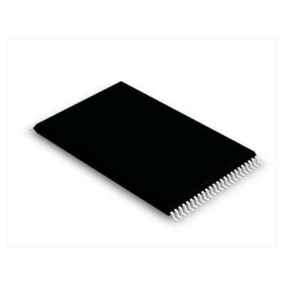
Buffer 2-CH Non-Inverting CMOS 6-Pin TSOP T/R


Images are for reference only.
See Product Specifications for product details.
Buffer 2-CH Non-Inverting CMOS 6-Pin TSOP T/R
Orders over $200 are eligible for a limited edition Chinese-style gift.
Orders over $1000 qualify for a $30 shipping fee waiver.
Orders surpassing $5000 enjoy waived shipping and transaction fees.
These offers are applicable to both new and existing customers and are valid from January 1st, 2024, to December 31st, 2024.
NXP
74LVC2G34GV.125 datasheet
TSOP
IC Chips
 Lead free/RoHS Compliant
Submit your quote request now, and we expect to provide a quote within April 20, 2024. Place your order now, and we expect to complete the transaction within April 24, 2024. Ps:Time is according to GMT+8:00.


ZLG
3374 PCS
ZY2405WRBS-2W .PDF
POWERONE
3947 PCS
ZY1015G-Q1 .PDF
DIODES,ZETEX
3179 PCS
ZXTN5551FTA .PDF
ZETEX
647 PCS
ZXTN3035CLP-7B .PDF
2024-04-19
exelent very good service and good quality parts
2024-04-18
ótima qualidade
2024-04-18
Arrived quickly, good quality, would deal with again.
2024-04-17
GOOD+++++++++++++++++++++
2024-04-15
perfetto aticolo come da descrizione consegna vlocissima.
2024-04-12
Prodotto ok. FEDEX mai più. Spese doganali il doppio del valore della merce
2024-04-05
New and original, Good item
2024-03-23
Worked with my needs and came through for us. Nice to have suppliers this good.
2024-02-25
We highly recommend.
2024-01-03
we bought from censtry in April 2014, excellent transaction, Hardy-Pegasus
We highly value your feedback. Please share your most genuine review.
*Kindly log in to your account before posting a comment