Clock Drivers & Distribution ISP 0 Delay Unv Fan- Out Buf-Sngl End I


Images are for reference only.
See Product Specifications for product details.
Clock Drivers & Distribution ISP 0 Delay Unv Fan- Out Buf-Sngl End I
Orders over $200 are eligible for a limited edition Chinese-style gift.
Orders over $1000 qualify for a $30 shipping fee waiver.
Orders surpassing $5000 enjoy waived shipping and transaction fees.
These offers are applicable to both new and existing customers and are valid from January 1st, 2024, to December 31st, 2024.
Lattice
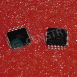
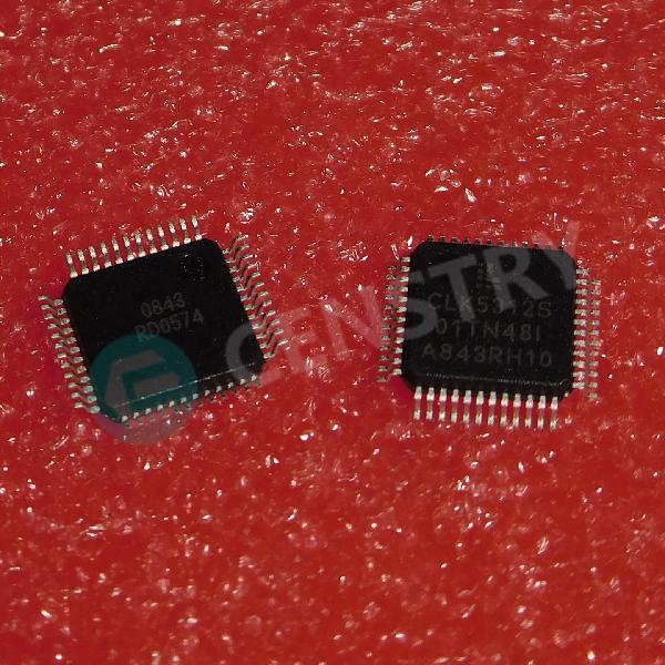
ISPPAC-CLK5312S-01TN48I datasheet
QFP-48
Clock & Timer Ics
Submit your quote request now, and we expect to provide a quote within April 20, 2024. Place your order now, and we expect to complete the transaction within April 24, 2024. Ps:Time is according to GMT+8:00.


Features
■ Four Operating Configurations
• Zero delay buffer
• Zero delay and non-zero delay buffer
• Dual non-zero delay buffer
• Non-zero delay buffer with output divider
■ 8MHz to 267MHz Input/Output Operation
■ Low Output to Output Skew (<100ps)
■ Low Jitter Peak-to-Peak (< 70 ps)
■ Up to 20 Programmable Fan-out Buffers
• Programmable single-ended output standards and individual enable controls
- LVTTL, LVCMOS, HSTL, eHSTL, SSTL
• Programmable output impedance
- 40 to 70Ω in 5Ω increments
• Programmable slew rate
• Up to 10 banks with individual VCCO and GND
- 1.5V, 1.8V, 2.5V, 3.3V
■ Fully Integrated High-Performance PLL
• Programmable lock detect
• Three “Power of 2” output dividers (5-bit)
• Programmable on-chip loop filter
• Compatible with spread spectrum clocks
• Internal/external feedback
■ Precision Programmable Phase Adjustment (Skew) Per Output
• 8 settings; minimum step size 156ps
- Locked to VCO frequency
• Up to +/- 5ns skew range
• Coarse and fine adjustment modes
■ Up to Three Clock Frequency Domains
■ Flexible Clock Reference and External Feedback Inputs
• Programmable single-ended or differential input reference standards
- LVTTL, LVCMOS, SSTL, HSTL, LVDS, LVPECL, Differential HSTL, Differential SSTL
• Clock A/B selection multiplexer
• Programmable Feedback Standards
- LVTTL, LVCMOS, SSTL, HSTL
• Programmable termination
■ All Inputs and Outputs are Hot Socket Compliant
■ Full JTAG Boundary Scan Test In-System Programming Support
■ Exceptional Power Supply Noise Immunity
■ Commercial (0 to 70°C) and Industrial (-40 to 85°C) Temperature Ranges
■ 48-pin and 64-pin TQFP Packages
■ Applications
• Circuit board common clock distribution
• PLL-based frequency generation
• High fan-out clock buffer
• Zero-delay clock buffer
General Description
The ispClock5300S is an in-system-programmable zero delay universal fan-out buffer for use in clock distribution applications. The ispClock5312S, the first member of the ispClock5300S family, provides up to 12 single-ended ultra low skew outputs. Each pair of outputs may be independently configured to support separate I/O standards (LVTTL, LVCMOS -3.3V, 2.5V, 1.8, SSTL, HSTL) and output frequency. In addition, each output provides independent programmable control of termination, slew-rate, and timing skew. All configuration information is stored onchip in non-volatile E2 CMOS® memory.
The ispClock5300S devices provide extremely low propagation delay (zero-delay) from input to output using the on-chip low jitter high-performance PLL. A set of three programmable 5-bit counters can be used to generate three frequencies derived from the PLL clock. These counters are programmable in powers of 2 only (1, 2, 4, 8, 16, 32). The clock output from any of the V-dividers can then be routed to any clock output pin through the output routing matrix. The output routing matrix, in addition, also enables routing of reference clock inputs directly to any output.

Request a quote ISPPAC-CLK5312S-01TN48I at censtry.com. All items are new and original with 365 days warranty! The excellent quality
and guaranteed services of ISPPAC-CLK5312S-01TN48I in stock for sale, check stock quantity and pricing,
view product specifications, and order contact us:[email protected].
The price and lead time for ISPPAC-CLK5312S-01TN48I depending on the quantity required, please send your request to us,
our sales team will provide you price and delivery within 24 hours, we sincerely look forward to cooperating with you.
ZLG
3374 PCS
ZY2405WRBS-2W .PDF
POWERONE
3947 PCS
ZY1015G-Q1 .PDF
DIODES,ZETEX
3179 PCS
ZXTN5551FTA .PDF
ZETEX
647 PCS
ZXTN3035CLP-7B .PDF
2024-04-19
Great company, nice people, professional ... Thanks to Robin
2024-04-19
Great supplier!
2024-04-19
Great people, great company
2024-04-18
GREAT SUPPLIER ALWAYS DELIVERS ON TIME WITH PRODUCT IN PERFECT CONDITION I WILL ALWAYS BUY FROM THIS COMPANY
2024-04-17
John & Censtry Electronics are A+++
2024-04-14
Highly Recommend Censtry Chips
2024-04-09
I have bought some switches from them. The package was beautiful and the parts were 100% perfect. Thank you.
2024-03-29
Issue resolved
2024-03-08
Jason is the MAN. I had a small crystal order that is crucial to my OEM. Jason went out of his way to get them confirmed & to help me out tremendously. THANK YOU FOR YOUR HARD WORK!!!! We appreciate it & will be giving you as much biz as we can in the future!!!! Thanks Jason!!!!!
2024-01-25
June and Camille are pros, great customer & a joy to work with, we look forward to the next opportunity ;-)

We highly value your feedback. Please share your most genuine review.
*Kindly log in to your account before posting a comment